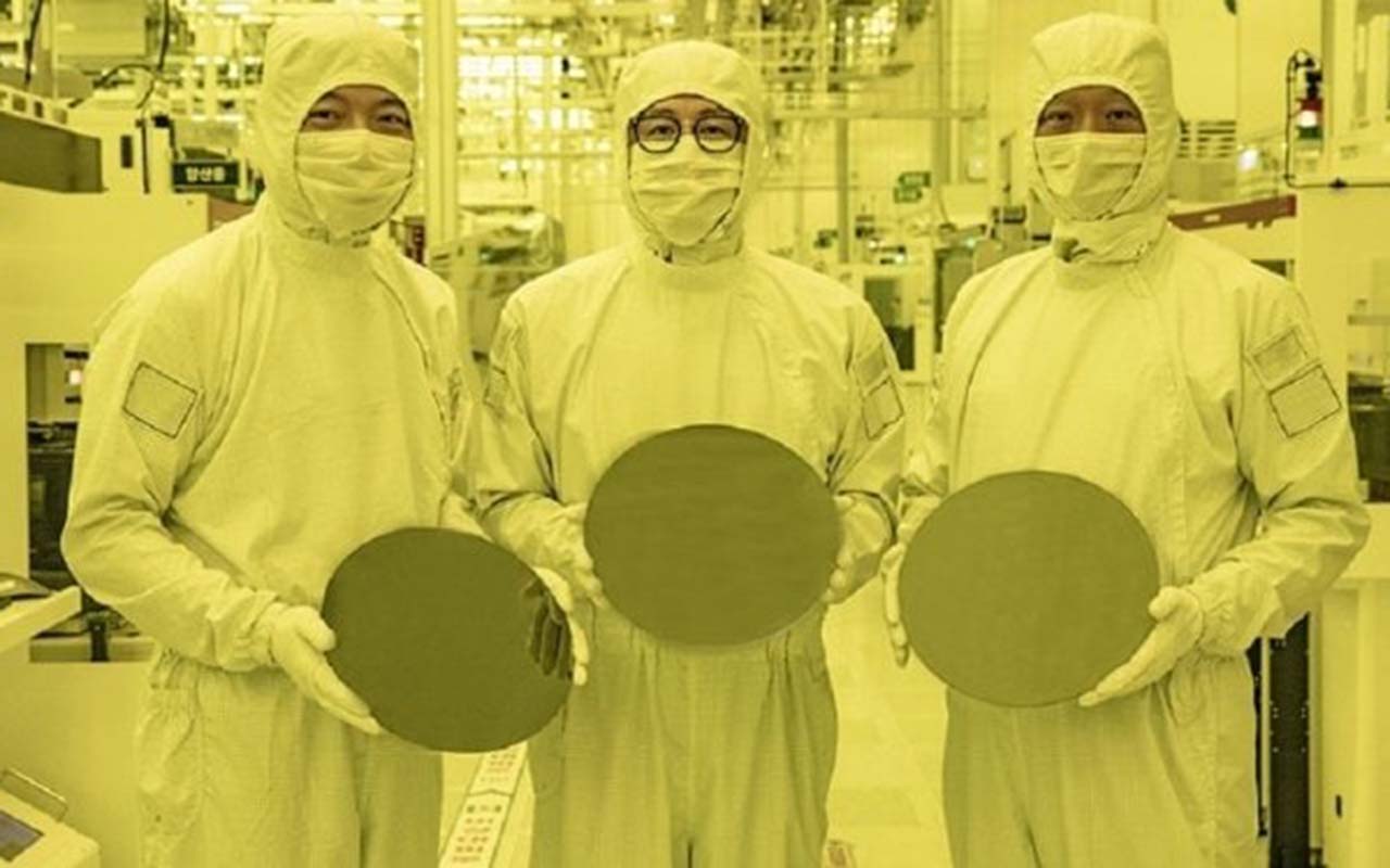
Gadgets will become 30% more powerful. Samsung launches production of 3nm chips
Samsung has begun mass production of chips on a more advanced 3-nanometer process technology. The company spoke about the advantage of the technology on its official website.
Compared to the 5nm process, the first-generation 3nm process should reduce power consumption by 45%, improve performance by 23%, and reduce wafer area by 16%. At the same time, the second generation makes it possible to make chips 50% more economical, 30% more powerful and 35% smaller. It is noteworthy that the main competitor of Samsung, the Taiwanese company TSMC, plans to mass-produce 3-nm chips only in the third quarter of 2022.
South Korean developer Samsung has implemented a transistor architecture with a circular arrangement of gates (Gate-All-Around). Nanosheets with wider channels are used as plates, increasing productivity and energy efficiency compared to nanowires with narrower channels. Designers will be able to adjust the nanosheet’s channel width to optimize performance for different needs. Multi-Bridge-Channel FET (MBCFET) technology further improves energy efficiency by lowering supply voltage levels, and performance by increasing drive current capability.
First of all, Samsung uses its nanosheet semiconductor chips for high-performance computing applications. In the near future, they plan to introduce them into mobile processors, which should make smartphones even more powerful and autonomous.
“Samsung is growing rapidly as we continue to lead the way with next-generation technologies such as the foundry’s first High-K metal gates, FinFET, and EUV. We aim to maintain this leadership with the world’s first 3nm MBCFET process,” Sieng Choi, president and head of foundry at Samsung Electronics, commented.
Tom Beckley, senior vice president of Cadenc, noted that Samsung’s chips incorporate his company’s digital solutions, such as Cadence Cerebrus technology, which improves performance through artificial intelligence. Synopsys General Manager Shankar Krishnamurthy added that the 3nm process is being tested in Synopsys Digital Design, Analog Design and IP products, which will help manufacturers develop different chips based on the new chips.